Pomegra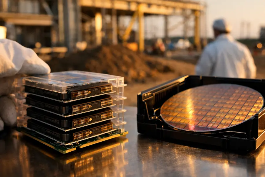
SK Hynix's $4 billion West Lafayette facility - the first U.S.-based HBM packaging plant - locks in American AI chip supply chain resilience with volume HBM4E production targeted for Q3 2029.
- SK Hynix (SKHY) broke ground August 27 at Purdue Research Park on a 133.5-acre advanced packaging facility funded in part by $458 million in CHIPS Act grants.
- The plant will supply Nvidia (NVDA) and other hyperscalers with domestically packaged HBM4E, the next-generation AI memory format, beginning Q3 2029.
- SK Hynix controls approximately 58% of the global HBM market by revenue and supplies roughly two-thirds of Nvidia's HBM4 chips.
Lead
SK Hynix held a ceremonial groundbreaking on August 27, 2026 at Purdue Research Park in West Lafayette, Indiana, launching construction of a $4 billion advanced memory packaging and testing facility - the first of its kind on American soil. The 133.5-acre campus will receive DRAM wafers from South Korea for stacking, packaging, and testing into high bandwidth memory modules, with cleanroom operations scheduled to begin in Q4 2028 and volume production of HBM4E chips targeting Q3 2029. The project, backed by $458 million in federal CHIPS Act grants and up to $700 million in Indiana state incentives, is the largest single memory-infrastructure investment in U.S. history.
What Does the Indiana Plant Actually Produce?
The West Lafayette facility is not a wafer fabrication plant but an advanced packaging hub - the final, technically demanding stage where DRAM dies are stacked vertically using through-silicon vias and interconnected at extreme precision to form HBM modules. This packaging process is distinct from chip manufacturing and has historically been concentrated in South Korea and Taiwan. By relocating it to the United States, SK Hynix inserts a domestic node into what has been an entirely offshore supply chain for the AI memory that powers data center GPU clusters. At full capacity, the site is expected to produce hundreds of thousands of packaged wafers annually, supporting roughly 1,000 direct jobs and an estimated 7,000 positions including construction, operations, and supplier activity.
Why Is This Project a Geopolitical Priority?
HBM has emerged as a hard chokepoint in global AI infrastructure. Nvidia's GPU platforms - including the Blackwell and next-generation Rubin architectures - require HBM stacks that cannot be substituted or sourced from commodity memory channels. Until the West Lafayette plant reaches production, every HBM module in an American data center is packaged in East Asia. That geographic concentration represents a structural vulnerability that both Washington and Seoul have moved to correct. The CHIPS Act grant finalized in December 2024, combined with Indiana's $700 million incentive package, reflects a bipartisan recognition that HBM supply chain security is inseparable from national AI competitiveness. South Korea's government has similarly framed the investment as an extension of the U.S.-Korea technology alliance, with SK Hynix CEO Kwak Noh-Jung describing the facility as the beginning of a "new future for U.S.-Korea AI."How Does Nvidia Factor Into the Business Case?
Nvidia's demand trajectory is the load-bearing assumption beneath the entire $4 billion commitment. In June 2026, Nvidia and SK Hynix formalized a multi-year technology partnership covering Nvidia's full forward product roadmap, locking in HBM supply agreements through at least 2030. SK Hynix already supplies approximately two-thirds of Nvidia's HBM4 requirements, and from the HBM4E generation onward, the company is pivoting to a fully customized production model tailored to individual customer specifications - a shift that makes co-location with U.S. customers strategically valuable, not merely symbolic. Nvidia shares rose more than 5% on August 26 following the company's Q2 earnings report, which included a forecast of a 70% revenue jump for the next fiscal year, reinforcing the demand signal that underpins SK Hynix's Indiana bet.
Strategic Context: Competition and Consolidation
SK Hynix's move sets the terms for competitive response across the HBM landscape. Micron Technology (MU) is the only other HBM supplier with a meaningful U.S. manufacturing base, and its HBM3E ramp has lagged SK Hynix in both volume and customer adoption. Samsung, the third major HBM producer, has struggled with yield issues on advanced stacks and has not announced a comparable U.S. packaging investment. The Indiana facility - alongside the June Nvidia partnership - effectively converts SK Hynix's technical lead into a structural supply chain advantage that competitors would require years to replicate. For investors tracking ai stocks, the consolidation of HBM supply around a single dominant partner with a domestic U.S. anchor represents a durable shift in sector economics, with downstream implications for semiconductor ETFs including SMH and SOXL.
CEO Warning: Memory Shortage Through 2030
At the groundbreaking, CEO Kwak Noh-Jung stated that the global memory shortage would persist through 2030, a projection consistent with demand forecasts tied to accelerating AI model training and inference workloads. The warning carries both supply-chain and investment implications: it signals that HBM pricing power is unlikely to erode in the medium term, and it frames the Indiana facility not as excess capacity but as a minimum-necessary build to keep pace with committed customer demand from Nvidia, Microsoft, Google, and Broadcom, all of which have placed custom AI memory orders with SK Hynix.
Outlook
The West Lafayette groundbreaking marks a structural inflection point in American semiconductor policy, converting CHIPS Act ambition into poured concrete. With cleanroom operations targeted for Q4 2028 and HBM4E volume production for Q3 2029, SK Hynix's Indiana campus will be operational during what the company itself projects as the deepest phase of the global memory shortage. Federal and state subsidies totaling over $1.15 billion reduce financial risk while cementing a U.S.-South Korea AI hardware alliance that both governments have elevated to a national security priority. The facility's success or delay will be a leading indicator for the broader thesis that advanced semiconductor packaging - not just chip design - can be anchored in the United States.