IBM's 0.7nm nanostack chip delivers 70% efficiency gains and 7,000 TOPS of AI compute, setting a new benchmark that could extend Moore's Law another decade.
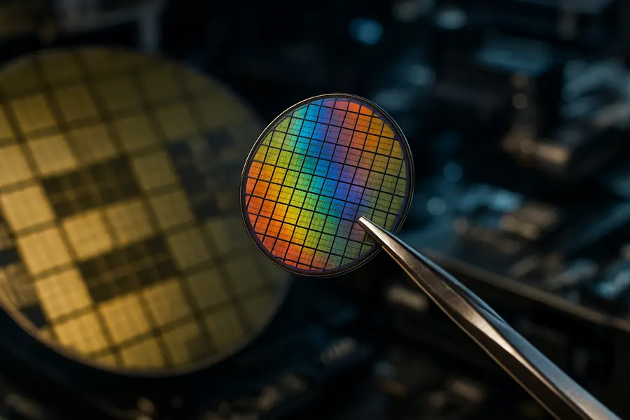
- IBM's 0.7nm nanostack chip packs ~100bn transistors, double its 2021 2nm density, with 50% more performance or 70% greater energy efficiency.
- AI accelerators on the 7-angstrom node could hit 7,000 TOPS vs. today's ~1,500, cutting large-model training from three months to roughly two weeks.
- Commercial production is five years out; no manufacturing partner is named, with IBM positioning itself as a research, licensing, and co-development operation.
Lead
International Business Machines (NYSE: IBM) on Thursday unveiled the world's first chip technology operating below the one-nanometer threshold, announcing a 0.7nm — or 7-angstrom — node built on a three-dimensional transistor design the company calls nanostack. IBM shares rose approximately 2% to around $69 in regular trading, pulling back from premarket gains of as much as 6%, as investors processed the scale of the engineering advance. The announcement, made through IBM Research, targets semiconductor customers, government labs, and AI infrastructure operators seeking a credible path to sustain computing density gains as today's leading-edge nodes approach physical limits.What Happened
IBM's nanostack design departs fundamentally from the planar and gate-all-around transistor geometries that define current leading-edge semiconductor production. Rather than arranging transistors in a single horizontal plane, the architecture stacks them vertically and staggers the upper layer relative to the lower — a configuration IBM describes as analogous to a block-of-flats layout. The staggered positioning simplifies interconnect routing and permits engineers to use different materials in each layer, allowing power and performance to be optimized independently.
The result is nearly 100 billion transistors on a fingernail-sized die — approximately double the density of IBM's 2nm chip first demonstrated in 2021. The 0.7nm node delivers up to 50% greater performance or 70% greater energy efficiency relative to that 2nm baseline, depending on workload configuration. IBM's collaboration with Lam Research, formalized in March 2026 as a five-year co-development agreement, is central to translating the architecture from research silicon into manufacturable processes. The two companies are jointly developing new materials and etch techniques required at the sub-1nm regime.
Market Reaction
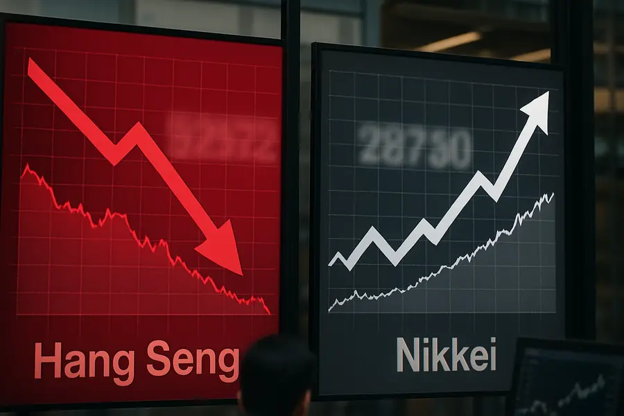
IBM shares settled near $69, reflecting a roughly 2% gain in the regular session after a sharper premarket move. The broader semis sector drew attention as investors weighed whether IBM's advance could catalyze a new investment cycle in advanced chip infrastructure. IBM has framed its commercialization approach around licensing and co-development rather than high-volume foundry capacity, following the model it established through technology agreements with Samsung and Japan's Rapidus — an approach that limits capital exposure while allowing partners to scale.
Strategic Context
The nanostack announcement positions IBM well ahead of the current commercial frontier. Intel has moved its 18A process — a 1.8nm node — into risk production, while TSMC recently began volume manufacturing of 2nm-class silicon. IBM's leap to 0.7nm represents a roughly two full-node advantage over what is in mass production today, though the five-year commercialization horizon means direct competitive pressure on existing foundry leaders remains prospective.
The architecture embodies a deliberate industry bet: that horizontal planar scaling is largely exhausted and that three-dimensional transistor integration is the route through which Moore's Law sustains another decade of density gains. If nanostack processes are reproduced by foundry partners, the design could reorder competitive dynamics among chip designers, hyperscalers, and defense customers reliant on the most advanced compute available.
AI and Technology Angle
IBM quantifies the AI implications directly. Accelerators built on the 7-angstrom node are estimated to reach approximately 7,000 TOPS (trillions of operations per second), compared with roughly 1,500 TOPS on current leading hardware. Applied to large-model training, that density advantage compresses multi-month runs to roughly two weeks — a meaningful reduction for cloud operators paying for GPU time and energy at scale.
IBM's chief executive has previously flagged that the AI data-center buildout is approaching unsustainable infrastructure cost trajectories. The sub-1nm chip addresses that pressure directly: denser, more efficient silicon lowers the capital and operating cost per unit of compute. Energy efficiency gains carry additional weight as data centers across key markets contend with power-capacity constraints that are already constraining AI expansion.
What Comes Next
IBM has not identified a manufacturing partner for the 0.7nm process, and volume production is targeted within five years — placing commercial availability closer to 2031. In the interim, the company's strategy centers on licensing the intellectual property, deepening the Lam Research materials collaboration, and integrating nanostack research into its high-performance computing and quantum roadmaps. Any manufacturing partnership discussions with non-U.S. foundries will intersect with U.S. export-control policy on advanced semiconductor technology, adding a geopolitical dimension to the commercialization path that IBM has not yet addressed publicly.
Outlook
IBM's sub-1nm announcement resets the density benchmark and establishes a credible architecture beyond the current 2nm frontier. The five-year production timeline and the absence of a named manufacturing partner introduce execution risk, but the nanostack design's simultaneous efficiency and performance gains position it as foundational for next-generation AI compute, government supercomputing, and next-decade data-center infrastructure. Licensing agreements and foundry partnerships will be the near-term metrics by which the market determines whether IBM's research lead converts into durable commercial value.
Technology }}