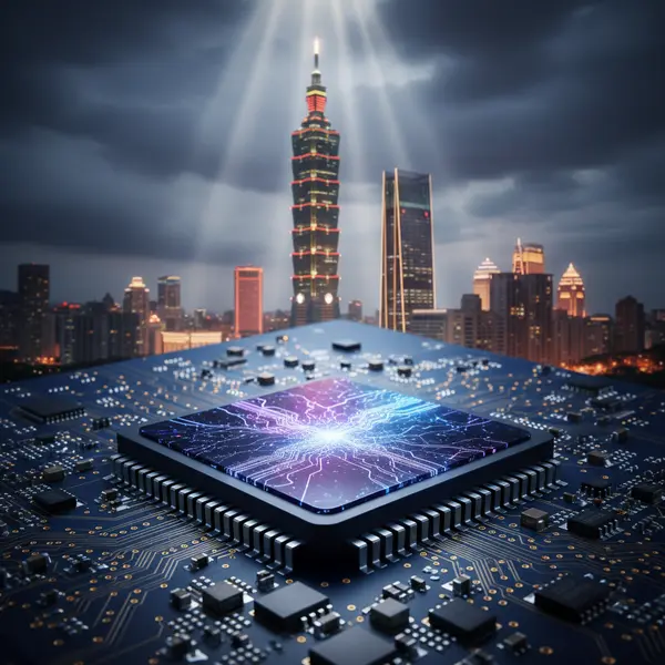
Advanced Micro Devices (NASDAQ: AMD) announced on May 21, 2026 a commitment of more than $10 billion across Taiwan's semiconductor ecosystem, pairing one of the largest chipmaker investment pledges of the year with a landmark manufacturing milestone: the production ramp of its next-generation EPYC processor, codenamed "Venice", on TSMC's advanced 2-nanometer process technology — the first high-performance computing chip in the world to reach production at that node.
- AMD commits more than $10 billion to Taiwan's chip ecosystem to scale advanced packaging and AI infrastructure partnerships.
- EPYC "Venice" becomes the first high-performance computing product in the industry to enter production on TSMC's 2nm process technology.
- AMD shares surged 8.10% following the announcement, reflecting strong market confidence in the AI infrastructure buildout.
A Historic Manufacturing Milestone for AI Computing
The Venice ramp represents the culmination of AMD's multi-year roadmap push into sixth-generation EPYC server processors, built on the Zen 6 architecture. Produced at TSMC's Taiwan fabrication facilities using the N2 nanosheet (Gate-All-Around FET) process, Venice delivers a step-change in transistor density, power efficiency, and raw compute throughput compared to prior generations. AMD has simultaneously confirmed future plans to ramp Venice production at TSMC's Arizona fabrication facility, extending its geographically diversified manufacturing footprint to U.S. soil.
TSMC Chairman and CEO Dr. C.C. Wei noted that the collaboration between AMD and TSMC represents the pairing of leadership process technology with advanced chip design to enable the next era of high-performance and AI computing — a strategic alignment that deepens one of the semiconductor industry's most consequential foundry relationships.
$10 Billion Committed to Taiwan's AI Ecosystem
The investment package extends well beyond a single chip. AMD's $10 billion commitment encompasses the expansion of strategic partnerships throughout Taiwan's advanced packaging supply chain, covering chiplet architectures, high-bandwidth memory (HBM) integration, 3D hybrid bonding, SoIC-X and CoWoS-L packaging technologies, and full rack-scale AI system design. The breadth of the commitment signals AMD's intent to compete aggressively at every layer of the AI infrastructure stack, from silicon to system.
CEO Dr. Lisa Su framed the announcement around the accelerating pace of global AI deployment: "As AI and agentic workloads scale rapidly, customers need platforms that can move from innovation to production faster. Our deep partnership with TSMC is helping AMD bring leadership compute technologies to market with the speed and scale required to meet this moment."
Agentic AI Drives CPU Demand
The timing of the Venice ramp is deliberate. As agentic AI workloads — systems in which AI models autonomously plan and execute multi-step tasks — proliferate across enterprise and cloud environments, the role of the CPU in the data center is being fundamentally re-evaluated. While GPUs handle parallel compute-intensive tasks, CPUs increasingly govern data orchestration, networking, security, and storage coordination across large-scale AI deployments.
AMD's EPYC platform has gained substantial traction in this environment, with rising customer adoption across cloud hyperscalers, enterprise infrastructure, high-performance computing (HPC) clusters, and AI-native deployments. The Venice ramp positions AMD to capitalize on this structural shift as customers upgrade server fleets to handle next-generation AI workloads.
The Road Beyond Venice: Verano
AMD also unveiled its follow-on 2nm product, codenamed "Verano" — a sixth-generation EPYC processor designed specifically for performance-per-dollar-per-watt leadership in cloud and AI environments. Verano will incorporate LPDDR memory integration, targeting the acute memory bandwidth constraints that define power-limited, agentic AI workloads. The expansion of the 2nm roadmap to include Verano underscores AMD's intent to dominate the server CPU segment through consecutive generational improvements on the same leading-edge node.
Market Reaction and Stock Performance
AMD shares responded sharply to the news, climbing 8.10% as of the announcement, with the stock trading at approximately $447.58, approaching its 52-week high of $469.21. The market capitalization of AMD reached $730 billion in the session, reflecting investor recognition of the company's deepening position in AI infrastructure hardware. Analyst consensus maintains a Buy rating on AMD shares, with an average price target of $446.76 — a figure already eclipsed by the day's gains.
TSMC's own shares traded at TWD 2,185.00 on the Taiwan Stock Exchange, with the foundry's market capitalization at approximately $1.794 trillion, as demand for its 2nm capacity continues to attract the largest names in global chip design.
Taiwan's Strategic Role in Global AI Infrastructure
AMD's $10 billion pledge adds to a growing chorus of major U.S. semiconductor companies reinforcing their commitments to Taiwan's chip manufacturing base, even as parallel investments in domestic U.S. fabs accelerate. The dual-track strategy — ramping in Taiwan today, scaling in Arizona tomorrow — reflects the industry's pragmatic approach to supply chain resilience: leveraging Taiwan's unmatched advanced manufacturing depth while building contingency capacity at home.
With TSMC already operating at the frontier of 2nm volume production and AMD now the first HPC company to achieve production ramp at that node, the competitive dynamics in AI silicon are entering a new phase. The combination of leading-edge process technology, aggressive packaging investment, and a deepening foundry partnership positions AMD as a formidable contender in the race to supply the backbone of global AI data center infrastructure through the remainder of the decade.
Mentioned tickers: AMD, TSM